AMD Rumours Are Flying Just Before The Big Reveal At Computex

It’s Just A Week Away
There is quite a bit of speculation about upcoming AMD products after several leaks hit the internet leading up to their big reveal at Computex, including Navi, Rome and the X570 chipset. Starting at the heart of the system, the new X570 chipset will be known as Valhalla and a diagram showed up over at TechPowerUp.

As you can see in the diagram above, there are a total of 28 lanes of the much anticipated PCIe 4.0 of which 16 are reserved for your GPU slots and from the leak another eight will be dedicated to a pair of M.2 slots. The rest will offer GbE and WiFi connectivity, a wide variety of USB ports and the ASMedia ASM1143 onboard audio. All that power does come with a drawback, the TDP of this chipset is reported to be three times higher than the previous generation; 15W will likely require some active cooling.
The second leak comes from WCCFTech and concerns the new Navi XT and Navi Pro cards, which they have dubbed the RX 3080 and RX 3070 for obvious reasons. The RX 3080 is suggested to be slightly faster than NVIDIA’s RTX 2070 and should sport an MSRP of $499, while the performance of the RX 3070 should fall in between the RTX 2060 and 2070 and is expect to come with a $399 price tag. The price makes sense for the Navi XT, as it matches the competition reference card pricing and one could reasonably expect the overclocked models to be similar. As long as the performance of the Navi Pro is closer to an RTX 2070 than the 2060 it’s price is also in line with the current market. We’ve heard previous rumours that this generation will bring ray tracing to AMD’s GPUs; which is why it is very interesting that the post concludes with a prediction that there will not be any dedicated ray tracing hardware on these cards. We should find out for sure in early July.
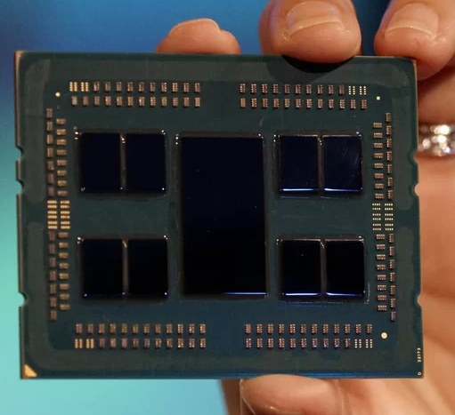
Finally, we have more Rome results thanks to another SiSoft Sandra results page which The Register heard word of and posted about. The results show a different processor than the original leak, this one sports 32 cores and 64-threads with a base frequency of 1.7GHz, turbo of 2.4GHz, with 16MB of L2 cache and 128MB of L3. The clock speeds are lower than the current 32 core EPYC, possibly due to the likelihood this is an engineering sample but could possibly reveal a side effect of moving to a 7nm process for the first time. The performance was impressive nonetheless, with the overall Sandra score ranking this mysterious second generation EPYC chip in 631st place globally.
Some, or all of these rumours will be revealed as truth or fiction on May 27th so stay tuned.
The spokesperson confirmed that AMD is in fact planning to announce two Radeon RX Navi graphics cards, code named Navi XT and Navi Pro . AKA the AMD Radeon RX 3080 and Radeon RX 3070. The announcement is allegedly coming as early as next week on Monday, the 27th of May.
More Tech News From Around The Web
- A Look At The MDS Cost On Xeon, EPYC & Xeon Total Impact Of Affected CPU Vulnerabilities @ Phoroni
- Intel Performance Hit 5x Harder Than AMD After Spectre, Meltdown Patches @ Slashdot
- Security boffins uncover Linux variant of Winnti malware @ The Inquirer
- Sophos tells users to roll back Microsoft’s Patch Tuesday run if they want PC to boot @ The Register
- Fun With Negative Resistance II: Unobtanium Russian Tunnel Diodes @ Hackaday
- Let adware be treated as malware, Canuck boffins declare after breaking open Wajam ad injector @ The Register
- How CPUs are Designed, Part 3: Building the Chip @ Techspot
- ASUS ROG Rapture GT-AC2900 Gaming Router @ Guru of 3D


I have been waiting for Zen 2 to build a new system for a while now. I don’t know what video card I am going to pair with it though. I am not really a gamer, so spending a lot on it will be a bit of a waste. I haven’t been to impressed with the enthusiast speculation and “analysis” unless I just haven’t come across some one who knows what they are talking about. I am expecting performance of Zen 2 to be very good, possibly with improved latency over Zen 1; hopefully worth the wait.
My speculation:
The cpu chiplets only have the cpu cores and a presumably 3 port infinty fabric switch. There is no memory clock on the cpu die, so it wouldn’t make much sense for the switch on the cpu chiplet to run at a different clock from the cpu cores. I would expect the switch to just run at core clock, so the connection between the two CCXs on each chiplet could be extremely fast. With low latency between the two on die CCXs, you should have good latency between 8 cores and 32 MB of L3 on die. Also, a 3-port switch at core clock is probably very low latency. It will still be a latency hit to go to the other chiplet for the 12 core and 16 core packages, but with infinity fabric running at ridiculously high clock, and possibly around 50 GB/s, I suspect the latency to the other chiplet to be quite good also.
AFAIK, Zen 1 uses 128-bit in each direction internally. This makes a lot of sense since a 64-bit DDR memory controller can deliver 128-bits per memory clock. The IFOP links are then essentially 1/4 the width at about 4x the clock and the IFIS links are essentially 1/8 the width at essentially 8x the memory clock. Everything matches nicely. They more than doubled the infinity fabric speed for Zen 2 though. Doubling the clock speed would probably take a lot more power so doubling the internal width to 256-bit may be more likely. That may explain why the Epyc Rome IO die is so large if internal paths are double the width compared to Zen 1. The memory clock is going to be higher but it also may be more likely that they will combine the two memory channels into essentially a single 128-bit DDR channel to provide the 256-bits per clock minimum. The diagrams for Zen 1 generally show 2 independent IF ports for the two memory controllers; see the ISSCC Zeppelin slides.
Even for local memory accesses, the data still needs to go through the fabric switch in Zen 1. The switch in Zen 1 has a lot of ports which may make it quite large, even at 128-bit width. The ISSCC slides show 11 ports on the fabric switch (2 CCX, 2 memory controllers, 4 IFOP, 2 IFIS, and 1 IOMS). The one in Ryzen 3000 may only be 5 or 6 ports. It would have 2 CCX (IFOP), 2 pci express (IFIS), and possibly just 1 memory controller port at 128-bits wide. The IO die for AM4 could also be simplified a bit since it doesn’t need to connect to other cpus. The IFIS style links could be pci express IO only. So it may be twice the width, it may have a lot less ports, and it may be designed to operate at a lot higher clock speed since much higher clock speed memory is supported. That all looks good for latency. It does have an extra off chiplet link to go through for local memory compared to Zen 1, but the infinity fabric link speed is very high, so latency of that link is probably quite low. Also, If they double the internal switch width, then It can essentially transfer cache lines in half the time.
I don’t know what they will do about ThreadRipper. The 16-core AM4 Ryzen 3000 part will probably outperform 16-core ThreadRipper except for possibly extremely memory bound applications. Zen 2 can probably support higher memory clock, so it may still do quite well though. This leaves ThreadRipper owners without a cpu upgrade. They could release a new ThreadRipper later, but it is probably very low priority compared to Rome.